Appendix B: Connector Pinouts
Pin-outs for all I/O connectors on the QScreen are provided here.
The QScreen Controller combines an embedded computer based on the 68HC11 microcontroller with a touch panel and LCD (liquid crystal display) graphic user interface (GUI) that is ideal for instrument control and automation.
QScreen Connectors
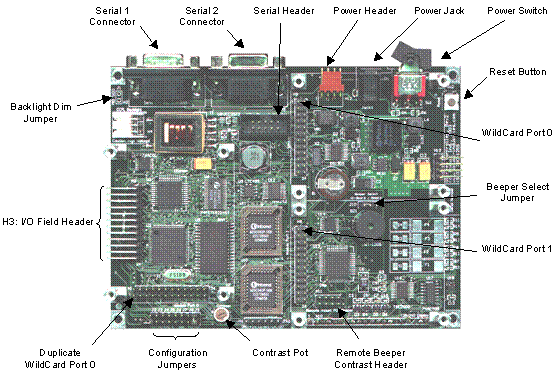
The pinouts of all of the connectors on the QCard Board are presented below. To locate the connectors on the board, consult Figure B–1 and the white silk–screened labels on the visible side of the QCard Board. The arrows in the figure point to the locations of pin 1 on each connector.
Figure B–1 QScreen Connectors, Headers, and Switches.
Table B-1 H12: Power Header
| Pin | Signal |
|---|---|
| 1 – | Vin |
| 2 – | GND |
| 3 – | +5v |
| 4 – | VBat |
Table B-2 H4: Serial Header
| Signal | Pins | Signal | |
|---|---|---|---|
| /TxD1 | – 1 | 2 – | /RxD1 |
| GND | – 3 | 4 – | GND |
| RS485 XCVR- | – 5 | 6 – | RS485 XCVR+ |
| /TxD2 | – 7 | 8 – | /RxD2 |
| GND | – 9 | 10 – | +5V |
Table B-3 H3: Field Header
| Signal | Pins | Signal | |
|---|---|---|---|
| GND | – 1 | 2 – | +5V |
| AGND | – 3 | 4 – | V+RAW |
| (/TxD2) /TxD1 | – 5 | 6 – | /RxD1 (/RxD2) |
| (/TxD2) XCVR- | – 7 | 8 – | XCVR+ (/RxD2) |
| PA7 | – 9 | 10 – | PA6 |
| PA5 | – 11 | 12 – | PA4/TxD2 |
| RxD2/PA3 | – 13 | 14 – | PA2 |
| PA1 | – 15 | 16 – | PA0 |
| AN7/PE7 | – 17 | 18 – | PE6/AN6 |
| AN5/PE5 | – 19 | 20 – | PE4/AN4 |
| AN3/PE3 | – 21 | 22 – | PE2/AN2 |
| AN1/PE1 | – 23 | 24 – | PE0/AN0 |
| Note: Signals in parentheses indicate options configured by installing appropriate zero ohm shorts on the board. | |||
Table B-4 H1,H8,H9: Wildcard Port Header
| Signal | Pins | Signal | |
|---|---|---|---|
| GND | – 1 | 2 – | +5V |
| /IRQ | – 3 | 4 – | V+RAW |
| SEL1/XMIT1 | – 5 | 6 – | SEL0/XMIT+ |
| MOSI/XCV- | – 7 | 8 – | MISO/XCV+ |
| /RESET | – 9 | 10 – | SCK |
| /MOD.CS | – 11 | 12 – | 16 MHz |
| E | – 13 | 14 – | R//W |
| /OE | – 15 | 16 – | /WE |
| AD7 | – 17 | 18 – | AD6 |
| AD5 | – 19 | 20 – | AD4 |
| AD3 | – 21 | 22 – | AD2 |
| AD1 | – 23 | 24 – | AD0 |
Table B-5 Serial 1 Connector
| Signal | Pins | Signal | |
|---|---|---|---|
| DCD1/DSR1/DTR1 | – 1 | ||
| 6 – | DSR1/DTR1/DCD1 | ||
| /TXD1 | – 2 | ||
| 7 – | CTS1 | ||
| /RXD1 | – 3 | ||
| 8 – | RTS1 | ||
| DSR1/DTR1/DCD1 | – 4 | ||
| 9 – | NC | ||
| DGND | – 5 | ||
| Notes: NC indicates no connection Pins 1, 4 and 6 (DCD1/DSR1/DTR1) are connected. Pins 7 and 8 (CTS1/RTS1) are connected. | |||
Table B-6 Serial 2 Connector
| Signal | Pins | Signal | |
|---|---|---|---|
| DCD2 | – 1 | ||
| 6 – | DSR2/DTR2/DCD2 | ||
| /TXD2 | – 2 | ||
| 7 – | CTS2/RTS2 | ||
| /RXD2 | – 3 | ||
| 8 – | RTS2/CTS2 | ||
| DSR2/DTR2/DCD2 | – 4 | ||
| 9 – | NC | ||
| DGND | – 5 | ||
| Notes: NC indicates no connection Pins 1, 4 and 6 (DCD2/DSR2/DTR2) are connected. Pins 7 and 8 (CTS2/RTS2) are connected. | |||
Table B-7 H11: Remote Contrast Beeper Header
| Signal | Pins | Signal | |
|---|---|---|---|
| GND | – 1 | 2 – | +5V |
| +5V | – 3 | 4 – | V+RAW |
| VCON- | – 5 | 6 – | VEE |
| GND | – 9 | 10 – | REMOTE_BEEPER |

