LCVR Controller Specifications
Nematic liquid crystal driver amplitude and frequency specifications
This liquid crystal controller provides a driver circuit that is compatible with all Liquid Crystal Variable Retarders (LCVRs) and is also ideal for driving most other nematic liquid crystal (LC) devices. This small electronic driver board provides a 2 kHz AC voltage to the LCVR with zero DC bias to prevent polarization and charge migration, which can otherwise limit LCVR device lifetime. The circuit's output frequency is jumper selectable and the drive amplitude is dynamically adjustable with high resolution.
The LCVR Driver Wildcard produces a slew rate limited, 2 kHz, symmetric square wave of programmable amplitude with a precisely controlled 50% duty cycle and zero DC component. The output voltage is programmable, and the frequency may be changed if needed. This LCVR driver may be used with any of Mosaic's microcontroller boards. It requires an analog voltage input, which can conveniently be generated from the DAC output of an Analog I/O Wildcard. The output of the LCVR driver is connected through a coax cable to the liquid crystal device or optical modulator.
The LCVR controller/driver circuit accepts an analog voltage input, Vin, in the range of 0=4.096V and converts it to a square wave magnitude of Vpeak = 2 Vin, or peak-to-peak magnitude of Vp-p = 4 Vin. The square wave's rise and fall times are slew rate limited to 1 μsec (as measured from zero crossing to full amplitude) to minimize overshoot and prevent cable ringing. The circuit's push-pull bipolar transistor output stage quickly charges and discharges cable and LCVR capacitance for fast switching.
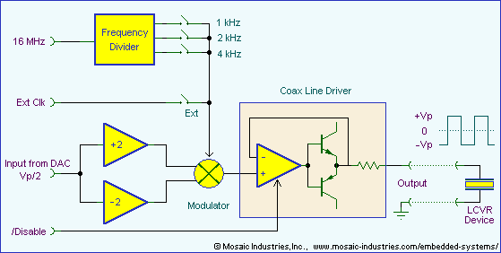
LC and LCVR controller schematic diagram
The following block diagram for the LCVR controller depicts the generation of a modulated square wave output from an amplitude-control analog voltage input:

The circuit's analog voltage input (generally taken from a DAC output of an Analog I/O Wildcard) is amplified and modulated to produce a square wave with a nominal frequency of approximately 2 kHz. The frequency is jumper selectable at appx. 1 KHz, 2 KHz or 4 KHz1), or an external logic-level frequency input may be used.
LC controller electrical and physical specifications
| Physical Specifications | |
|---|---|
| Weight | 20 gram |
| Footprint | Wildcard size, 2" × 2.5" × 0.415"2) |
| Power requirements | 5 VDC at 1 mA and 13.5 to 26 VDC at 12 mA from PDQ V+RAW, or, 5 VDC at 1 mA and 10.7 to 12.5 VDC at 12 mA from PDQ V+RAW (by installing R21) |
| Operating temperature | 0 to 50°C |
| Humidity | 5 - 95% RH noncondensing |
| Input characteristics | |
| Control Voltage | 0–2.048 or 0–4.096 V full scale (FS) from an Analog I/O Wildcard or other programmable voltage source |
| Control Voltage Input Impedance | 6 kΩ |
| Input Clock | If an external clock is supplied its logic levels must be: Input logic high: 3.5 to 5.0 V Input logic low: 0.0 to 1.0 V |
| Output characteristics | |
| Output form | Square wave with zero DC component |
| Output impedance | 5 Ω |
| Frequency | Default 1953.125 Hz, resistor selectable to 3906.25 or 976.5625 Hz, or externally driven |
| Frequency stability | ±100 ppm (-10°C to +70°C) ±5 ppm/year when using a 16 MHz clock from a Mosaic controller |
| Duty cycle | 50% ± several ppm measured from zero crossings |
| Amplitude and resolution | Vp = 0 to ± 4.096 V FS in 0.001 V steps, or 0 to ± 8.192 V FS in 0.002 V steps |
| Maximum average output current | ±30 mA |
| Rise/fall times | Slew rate limited, 1 μsec max from zero crossing |
| Slew rate | Limited to 8 V/μsec |
| DC offset | < 5 mV max (typically < 1 mV) < 1 mV when disabled |
| Overshoot | < 0.5 V (1st peak), < 3 μsec ring-down (< 1.5 typ.) for Vp =1 V, times measured from zero crossings |
| Maximum load capacitance | 100 nF |
| LCVR connector | PCB mounted, male contact, vertical RP-SMB jack 3) |
There are a few subtleties of the circuit's specifications:
- The DC offset is typically less than 1 mV for voltages up to Vpeak = 5 V. For greater voltages, there is a slight asymmetry of the output waveform's rise and fall times accounting for an effective DC offset of at most ±Vpeak/1000. The output is DC coupled.
- The gain of the board is precisely 2, so that Vpeak = 2 Vin. The voltage accuracy of the output magnitude is determined solely and entirely by the accuracy of the input voltage, which would normally be taken from a DAC output of an Analog I/O Wildcard.
Using the LCVR controller in an OEM scientific instrument
There are several analytical instruments that benefit greatly when using LCVRs or other inexpensive electrically switchable retardation plates. In particular, LCVRs allow producing inexpensive polarimeters, for high-precision spectropolarimetric measurements at very low cost. They are also used for fluorescence microscopy. In that case, a polarizer and a quarter-wave plate combined with a liquid crystal variable retarder allows tuning or rotating the angle of polarization of light prior to its illuminating a specimen in a fluorescence microscope.
For detailed instructions on installing, connecting to, and using this electronic controller for LCVRs, see the LCVR Controller User Guide.
