Power I/O Wildcard User Guide
The Power I/O Wildcard is an embedded I/O board that provides eight high-current, high voltage isolated DC outputs and four high voltage, isolated switch inputs. The outputs are provided by open-drain N-MOSFET transistors acting as solid state relays (SSRs). You can use the board within an instrument to control resistive or inductive loads, such as motors, solenoids, relays, heaters, fans and blowers, valves, high power LEDs or lamps.
This tiny 2" by 2.5" module is a member of the Wildcard™ series that connects to Mosaic embedded controllers, including the QCard Controller and the PDQ Boards.
This document describes the capabilities of the Power I/O Wildcard, tells how to use and configure the hardware, shows how to read the inputs and write to the outputs, and presents complete schematics.
Power I/O Wildcard hardware
The Power I/O Wildcard provides eight opto-isolated current-sinking outputs, and four opto-isolated high-voltage inputs. Jumpers enable board address selection and optional pull-up of the inputs. A Wildcard bus header connects to the host processor (e.g., PDQ Board, QScreen or QCard Controller), and a field header brings out the isolated I/O signals. The following table provides specifications for the module’s inputs and outputs.
Specifications
| Power I/O Wildcard Specifications | |
|---|---|
| High Current DC Outputs (each channel, without heat sink, TA = 0 to 70°C) | |
| Output Channels: | 8 isolated current sinking outputs with common field supply and ground |
| MOSFET SSR Used: | Rev_1a,b: IRLZ14 N-MOSFET (60V 10A) or Rev_1c: IPP230N06L3 N-MOSFET (60V 30A low ON resistance) |
| Isolation: | Optically isolated to ± 2500 V with 1011Ω isolation resistance |
| Output Protection: | Snub diodes to field supply to protect against inductive spikes |
| Field Voltage: | +5 to +50 VDC max |
| OFF Voltage: | +5 to +50 V (field supply) |
| OFF Leakage: | < 25 μA at 25° C |
| ON Voltage: | <0.08 V typical at 2 A (Rev_1c) |
| Max ON Resistance: | Rev_1a,b: <0.2 Ω at I < 1A, typically 0.15 Ω <0.3 Ω to <0.4 Ω (at I = 2A for TA = 25 to 70°C) Rev_1c: <0.040 Ω at I < 10A, typically 0.027 Ω |
| Max ON Current: | Rev_1a,b: 2 A continuously; or, 2 A pulses from 25 V at 50% duty cycle at frequencies to 5 KHz; or, 10 A pulse (<50 msec on time, <6% duty cycle at TA = 25°C or <4% duty cycle at TA = 70°C). Rev_1c: If outputs are soldered, 6A continuously, or 5A at frequencies to 5 KHz and voltages to 50V. If IDC connectors are used, max current capability of the cable and socket is 3A for isolated outputs, or 1.5A for all outputs simultaneously. |
| Switching Times: | Rev_1a: ton = 9 μsec, toff = 12 μsec for 10%-90% transitions Rev_1b,c: ton(fall time) = 0.5 μsec, toff(rise time) = 1 μsec for 10%-90% transitions ton_delay = 2 μsec, toff_delay = 39 μsec |
| Voltage / Switch Inputs (each channel) | |
|---|---|
| Input Channels: | 4 isolated bipolar voltage or switch closure inputs, with a common field ground and optional pull-ups to a common field supply |
| Input High Voltage: | ± 4 to ±50 VDC |
| Input Low Voltage: | < ± 0.8 V |
| Switch Inputs: | Optionally pulled-up through 10kΩ to field supply |
| Isolation: | Optically isolated to ± 2500 V with 1011Ω isolation resistance |
| Physical Specifications | |
|---|---|
| Current: |  mA from the Wildcard Bus +5V mA from the Wildcard Bus +5V |
| Weight: | 39 gram |
| Size: | 2" x 2.5" x 0.75" (50.8mm x 63.5mm x 19mm) |
Plugging in the Power I/O Wildcard
With the power off, connect the 24-pin Module Bus on the Power I/O Wildcard to Module Port 0 or Module Port 1 on your Mosaic controller. The corner mounting holes on the module should line up with the standoffs on the controller. The module ports are labeled on the silkscreen of the controller. Note that the Power I/O Wildcard headers are configured to allow direct stacking onto a controller, even if other modules are also installed. Do not use ribbon cables to connect the Power I/O Wildcard to the controller. Use of ribbon cables on the Power I/O Wildcard’s field header, however, is fine.
Selecting a board address
Once you have connected the Power I/O Wildcard to a controller, you must set the address of the module using jumper shunts across J1 and J2.
The address select jumpers, labeled J1 and J2, select a 2-bit digital code that sets a unique address on the Wildcard port of the controller. Each Wildcard port accommodates up to 4 Wildcards. Wildcard Port 0 provides access to Wildcard addresses 0-3 while WildcardPort 1 provides access to Wildcard addresses 4-7. Two Wildcards on the same port cannot have the same address (jumper settings). The following table shows the possible jumper settings and the corresponding addresses.
| Address Jumper Settings | ||
|---|---|---|
| Wildcard Port | Wildcard Address | Installed Jumper Shunts |
| 0 | 0 | None |
| 0 | 1 | J1 |
| 0 | 2 | J2 |
| 0 | 3 | J1 and J2 |
| 1 | 4 | None |
| 1 | 5 | J1 |
| 1 | 6 | J2 |
| 1 | 7 | J1 and J2 |
| Note:<block indent>Address 0 is not available on the QScreen or Handheld. Use addresses 1 through 7 instead.</block> | ||
Setting outputs and reading inputs
Once the wildcard address is established by setting the jumpers on the Wildcard, you can output data to the high current outputs, or input data from the inputs simply by writing or reading a single byte (char) from hexadecimal offset 0x00 and 0x01 using IOStoreChar and IOFetchChar. For example, if the wildcard address is set to 3, you can set all the outputs simultaneously by storing the desired output byte to offset 0x00 on wildcard 3
IOStoreChar( desiredOutput, 0x00, 3 );
or read the inputs by fetching a byte from offset 0x01 on wildcard 03.
IOFetchChar( 0x01, 3 );
An output is turned ON, that is, set to a low-voltage, current-sinking output state by writing a one to the corresponding bit of the output byte at offset 0x00. To change only a single, or several, output lines without affecting the others use the software primitives IOSetBits, or IOClearBits as described below.
Connecting high-current loads to the outputs
The high current MOSFET outputs are opto-isolated from the microcontroller side to 2500 volts and capable of sinking 2 amps per channel continuously using field voltages up to 50 VDC at ambient temperatures to 70°C. The outputs are protected by snub diodes connected to the field supply to prevent damage from high-voltage inductive spikes. The MOSFET outputs control DC loads only. To control AC loads, use the AC Relay Wildcard.
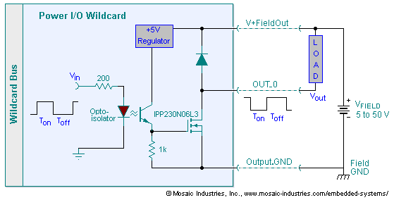
The simplified schematic1) of Figure 1 shows how the board's opto-isolated low side driver, an open-drain MOSFET2), connects to your external circuitry, including the field supply and electrical load.

Although the schematic of Figure 1 shows connections for only a single output, OUT_0, you may connect as many as eight outputs simultaneously. The DC load, for example a motor, solenoid, blower fan, or heater, may be inductive; in that case the board's internal fly-back diode protects the MOSFET from induced high voltage. For it to work properly, you must connect the field supply to the board. The field voltage supply, V+FieldOUT, can be as great as 50 VDC, and it must be at least 5 V to provide gate bias for the output MOSFETs.
If you test the MOSFET outputs, remember to connect a load to the output in order to see a voltage change as the output changes state. To perform simple non-isolated testing to verify the functionality of the board, connect a resistor (say, 1 kΩ) between the output and any convenient field supply (such as +5V) and connect the output’s field ground to the Ground connection of the +5V supply. Then, when an output bit is off, no current will flow in the load resistor, and a voltmeter or scope will show that its voltage is high (at +5V if you used this as the field supply). If you use the software from the software section of this document to turn an output bit on, current will flow through the output resistor, and your voltmeter or scope will show that the corresponding voltage falls to near zero.
Power I/O Wildcard field header
The isolated high voltage inputs and outputs are brought out to a 24-pin dual row header on the Power I/O Wildcard as shown in the following table.
| Power I/O Wildcard Field Header | |||
|---|---|---|---|
| Signal | Pins | Signal | |
| 0utput.GND | – 1 | 2 – | OUT7 |
| 0utput.GND | – 3 | 4 – | OUT6 |
| 0utput.GND | – 5 | 6 – | OUT5 |
| 0utput.GND | – 7 | 8 – | OUT4 |
| 0utput.GND | – 9 | 10 – | OUT3 |
| 0utput.GND | – 11 | 12 – | OUT2 |
| 0utput.GND | – 13 | 14 – | OUT1 |
| 0utput.GND | – 15 | 16 – | OUT0 |
| V+FieldOUT | – 17 | 18 – | IN3 |
| V+FieldIN | – 19 | 20 – | IN2 |
| Input.GND | – 21 | 22 – | IN1 |
| Input.GND | – 23 | 24 – | IN0 |
You'll notice that there is an additional output ground pin dedicated to each output line. You should use the output lines and their grounds in pairs, so that each ground line carries the current for its output pin. The ground lines should return the current to the negative side of your field supply. I you pulse width modulate an output, consider using a twisted pair cable if possible to carry the output line current and its ground line current.
To connect your transducer signals or control inputs to the Field Bus (H3 on the Power I/O Wildcard) use a ribbon cable or the Screw Terminal Module that brings out the signals to screw terminal blocks. Remember that most ribbon cable connectors are rated at 1 amp per contact. If you need more current, consider Mosaic's high current ribbon cable connector, part number IDC24-26AWG-24IN. Using it, you can switch up to 4.5A rms using a single, isolated pin (with all the ground lines together carrying the return current), or you can switch up to 1.5A rms on all eight outputs together. For a discussion of the current handling capacity of ribbon cables and IDC sockets, see Ribbon Cable Current Rating.
Maximum ratings: current, power and switching frequency
If wires are soldered to the board in place of the field header, the outputs can each sink up to 6 A continuously. They can also sink pulses of greater current (up to 10 A) as long as the pulse duration and frequency do not cause a greater power dissipation than 6 A of continuous current does. At output switching frequencies up to 5 KHz and voltages to 50V each output can control up to 5A, if you solder wires to the board in place of ribbon cable connectors.
If you use standard IDC (ribbon cable) connectors , the allowed current is limited to the maximum current capability of the ribbon cable and IDC socket, which can be as great as 3A for isolated outputs, or 1.5A for all outputs simultaneously, when using AWG26 ribbon cable, as discussed in detail here.
For readers interested in the subtleties of calculating the power dissipation in switching MOSFETs, the remainder of this section discusses the factors that determined the maximum current capability.
Owing to the low ON resistance of the MOSFETS the power dissipated in them is low: when OFF they are subjected to the field voltage but there is no current so no power is dissipated; when ON their internal resistance is low (typically 0.027 Ω) so the I2R power is also low.
Without a heat sink, the maximum electrical power allowed for each channel is limited by convection/conduction from the MOSFET’s TO-220 package, and depends on the ambient temperature, as shown in Eqn. 1. In the equation, Tjmax is the maximum junction temperature (175°C), TA is the maximum ambient temperature (0-70°C), and RΘ is the junction to ambient thermal resistance (62 °C/W for a TO-220 case). For an ambient temperature increasing from 25°C to 70°C, the maximum power that can be dissipated decreases from 2.4 W to 1.7 W.
The heat generated in the MOSFET comprises two terms, an I2R term and a frequency-dependent switching loss term, as given in Eqn. 2.
The first term is the product of the square of the ON current, the device resistance (rds = 0.04 Ω max at the max junction temperature and current), and the duty factor (0<D<1). The duty factor is the ratio of ON time to (ON + OFF) time if the channel is switched repeatedly. The duty factor is unity, (D=1), for continuous current. The second term represents switching loss incurred during the turn on and off transitions. It is the product of the frequency, F, the ON current and OFF voltage, I and V, and the sum of the ON and OFF transition times (1.5 μsec). There is either a 6 or a 2 in the denominator if switching resistive (use 6) or inductive (use 2) loads respectively. A load is considered inductive if its inductance, L, is greater than a threshold given by L > V toff /4I. For example, if I=2A and V=25V, the load is inductive if its inductance is greater than 25V * 1μsec / (4 * 2A) = 3.125 μH.
The conditions of maximum current, voltage and frequency are found by setting the maximum package dissipation equal to the electrical power as shown in Eqn. 3.
And substituting the appropriate constants, as,
in which I is in amps, V in volts, D is a fraction between 0 and 1, F is in kHz, and TA is in °C.
Eqn. 4 can be solved to find any of the parameters (I, V, D, F, TA) given the others.
Example 2, finding a maximum switching frequency: For driving a 1 A resistive load (I=1) from a field supply of 25 volts (V=25) with a duty cycle of 50% (D=0.5) at a maximum ambient temperature of TA=70°C, we find a maximum frequency, F, of 267 KHz, indicating that power dissipation limits do not constrain the maximum frequency allowed. However, this frequency is unattainable – he maximum frequency is otherwise limited by ON-time and OFF-time delays, to less than 25 KHz.
Example 3, finding a maximum switching frequency for an inductive load: For driving 1A into an inductive load (I=1) of 1 mH from a field supply of 25 volts (V=25) with a duty cycle of 50% (D=0.5) at a maximum ambient temperature of TA=70°C, we use the denominator of 2 in the above equation and find a maximum frequency, F, of 89 kHz. Again, the maximum frequency is not limited by power dissipation, but by ON-time and OFF-time delays, to less than 25 KHz.
Example 4, finding maximum duty cycle: PWM modulation of a thermoelectric cooler requires driving 4 A into the cooler at its minimum recommended frequency of 1 kHz from a 12 volt supply. The instrument must operate at ambient temperatures up to 70°C. That is, I=4, F=1kHz, V=12, and TA=70°C. We find that the maximum duty cycle is not limited, but may be as great as 100%.
Example 5, finding maximum current at a switching frequency: If an inductive load is driven at a high duty cycle from a high voltage supply the maximum current allowed may be limited by the maximum power dissipation allowed. Suppose the switching frequency is 10 KHz, the ambient temperature is 50 °C and the field supply voltage is 50V. Then, solving Eqn. 4 we find the current to be limited to less than 3.8A — still greater than that allowed by IDC connectors to the field header.
Heat sinking
Output timing considerations
If you use the Power I/O Wildcard to turn ON and OFF devices in a quasi-static way, you do not need to worry about small turn-ON and turn-OFF delays. However, if you use the board to pulse width modulate current into a device at high frequency, then turn ON time, turn OFF time, turn ON delay and turn OFF delay are important, and limit the maximum frequency of operation.
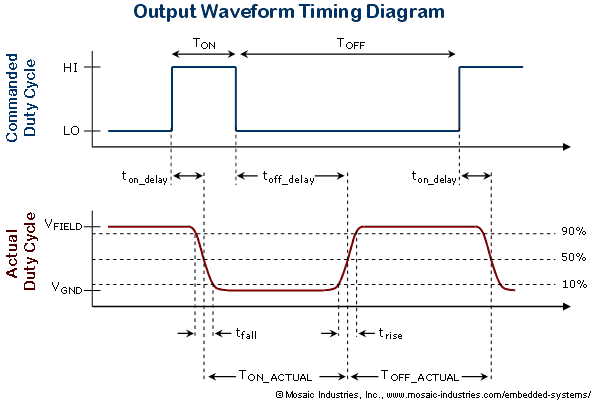
The following figure4) defines the turn ON/OFF delays and rise/fall times of the output waveform.

As shown in Figure 2, the commanded ON/OFF signal is an active high logic level. That is, to turn ON an output you write a logic 1 to the controlling bit. When the output turns ON, the output's open-drain MOSFET is turned ON, causing the output voltage to go low. The controlled load is placed between the output and the field supply voltage, so it is actuated by an output low.
| Turn ON/OFF Delays | |
|---|---|
| tON_delay | 2 μsec |
| tfall | .5 μsec |
| tOFF_delay | 39 μsec |
| trise | 1 μsec |
Turn on/off delays and rise times place a limitation on the effective maximum frequency of the PWM waveform of about 25 KHz. Owing to the longer delay in turning OFF than in turning ON, the ON time is lengthened beyond that commanded by about 37 μsec. The ON time lengthening is shown in Figure 2. Further, the sum of the delays and rise/fall times prevent commanding periods of less than about 40 μsec, corresponding to the maximum frequency of 25 KHz.
However, at that maximum limit there is no appreciable duty cycle range. The more important consideration is that whatever the frequency and duty cycle, the ON time is lengthened by 37 µsec so that the actual duty cycle produced is greater than that commanded. Consequently, the practical limitations are these:
- The commanded ON time must be greater than about 2.5 µsec for the device to turn fully ON.
- The commanded OFF time must be greater than 40 µsec for the device to turn fully OFF.
- The actual ON time produced is 37 µsec greater than that commanded, so the device is ON longer than expected during each cycle, introducing an error in the actual duty cycle produced, unless it is accounted for.
Connecting to the inputs
The high voltage inputs are also optically isolated to ±2500 volts and capable of sensing voltages of ±4 to ±50 VDC. Figure 3 illustrates how to connect an input voltage to the Power I/O Wildcard. When the input voltage is ±4 to ±50V, a logical 1 input will be read. When the input voltage is less than ±0.8V, a logical 0 input will be read.

Onboard pull-up resistors (labeled PU0 to PU3 on the Power I/O Wildcard silkscreen) allow you to monitor the state of a contact closure device such as a switch. The switch is connected as shown in Figure 4. For example, to interface a contact closure device to input channel IN1, install a jumper shunt across J5 and connect the contact closure device. The input is read as a logical 1 when the switch contact is open (contacts not connected), and it is read as a logical 0 when the device is closed (contacts connected). When the pull-up resistors are used, V+ Field IN must be in the range of ±4 to ±50VDC for proper operation.

Software
To use the eight high current, isolated MOSFET outputs for instrumentation, use the following software primitives for either the Forth or C programming languages:
| Using Forth | Using C |
|---|---|
| IO.C! | IOStoreChar |
| IO.CHANGE.BITS | IOChangeBits |
| IO.SET.BITS | IOSetBits |
| IO.CLEAR.BITS | IOClearBits |
| IO.C@ | IOFetchChar |
To read back the state of the eight outputs or the four inputs, use the software primitive IOFetchChar (IO.C@ in FORTH). The hexadecimal offset of the output port is 0x00 and the offset address of the input port is 0x01.
The following code examples set, clear, and read the high current isolated outputs; they also show a function that reads the high voltage isolated inputs.
C code to control the Power I/O Module.
A C language demo source code listing here is also located in your installation directory.
Forth code to control the Power I/O Module.
A Forth language demo source code listing here is also located in your installation directory.
Hardware schematics
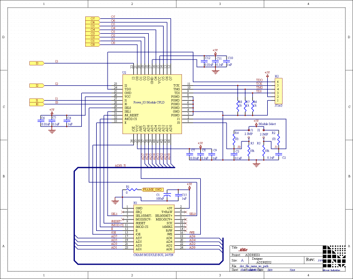
Schematic Page 1 as a pdf file
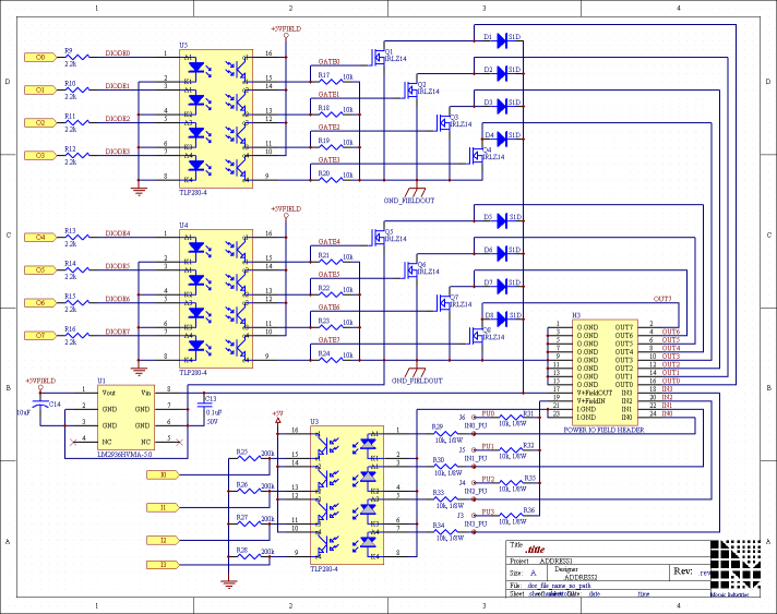
Schematic Page 2 as a pdf file
Several changes have been made to the board for revisions Rev_1b and Rev_1c that are not reflected on these schematics. Specifically, the MOSFETs have been changed to lower ON-resistance, higher current MOSFETs (PN IPP230N06L3) for Rev_1c; the MOSFET gate pull down resistors, R17 through R24, have been changed to 1K; and, the opto-isolator input resistors, R9 through R16, have been changed to 200 ohms. These changes provide quicker turn ON/OFF and greater current capability.
See also →


