Appendix B: Connector Pinouts
The QCard Controller Starter Kit comprises a stack of two boards: the PowerDock Board, and the smaller QCard Single Board Computer (SBC) based on the 68HC11 microcontroller. Pin-outs for all input-output (IO) connectors on the QCard Board and the PowerDock Board are provided here.
QCard connectors
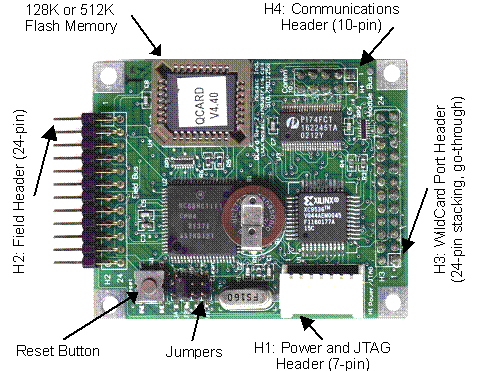
The pinouts of all of the connectors on the QCard Board are presented below. To locate the connectors on the board, consult Figure B–1 and the white silk–screened labels on the visible side of the QCard Board. The arrows in the figure point to the locations of pin 1 on each connector.
QCard Connectors and Switches. Arrows locate pin 1 of each header.
H1: Power Header
| Pin | Signal |
|---|---|
| 1 – | V+RAW (+8 to +26 VDC) |
| 2 – | GND |
| 3 – | +5 VDC |
| 4 – | TDI for JTAG programming |
| 5 – | TMS for JTAG programming |
| 6 – | TCK for JTAG programming |
| 7 – | TDO for JTAG programming |
| Note: V+RAW is needed only if certain WildCards are used. Pins 4-7 are generally not used. | |
H2: Field Header
| Signal | Pins | Signal | |
|---|---|---|---|
| GND | – 1 | 2 – | +5V |
| AGND | – 3 | 4 – | V+RAW |
| (/TxD2) /TxD1 | – 5 | 6 – | /RxD1 (/RxD2) |
| (/TxD2) XCVR- | – 7 | 8 – | XCVR+ (/RxD2) |
| PA7 | – 9 | 10 – | PA6 |
| PA5 | – 11 | 12 – | PA4/TxD2 |
| RxD2/PA3 | – 13 | 14 – | PA2 |
| PA1 | – 15 | 16 – | PA0 |
| AN7/PE7 | – 17 | 18 – | PE6/AN6 |
| AN5/PE5 | – 19 | 20 – | PE4/AN4 |
| AN3/PE3 | – 21 | 22 – | PE2/AN2 |
| AN1/PE1 | – 23 | 24 – | PE0/AN0 |
| Note: Signals in parentheses indicate options configured by installing appropriate zero ohm shorts on the board. | |||
H3: Wildcard Port Header
| Signal | Pins | Signal | |
|---|---|---|---|
| GND | – 1 | 2 – | +5V |
| /IRQ | – 3 | 4 – | V+Raw |
| SEL1/XMIT- | – 5 | 6 – | SEL0/XMIT+ |
| MOSI/XCV- | – 7 | 8 – | MISO/XCV+ |
| /RESET | – 9 | 10 – | SCK |
| /MOD.CS | – 11 | 12 – | 16 MHz |
| E | – 13 | 14 – | R/W |
| /OE | – 15 | 16 – | /WE |
| AD7 | – 17 | 18 – | AD6 |
| AD5 | – 19 | 20 – | AD4 |
| AD3 | – 21 | 22 – | AD2 |
| AD1 | – 23 | 24 – | AD0 |
H4: Communications Header
| Signal | Pins | Signal | |
|---|---|---|---|
| /TxD1 | – 1 | 2 – | /RxD1 |
| DGND | – 3 | 4 – | /MOD1.CS |
| RS485 XCVR- | – 5 | 6 – | RS485 XCVR+ |
| /TxD2 | – 7 | 8 – | /RxD2 |
| DGND | – 9 | 10 – | +VBAT |
| Note: This pinout matches that of the Docking Panel comm socket, but differs from the comm header (right-angle pins) on the Docking panel. On the docking panel comm header, pin 4 is connected to DGND and pin 10 is connected to +5V. | |||
PowerDock connectors
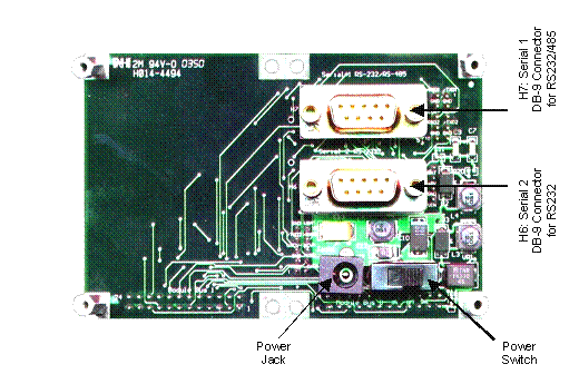
The pin-outs of all of the connectors on the PowerDock are presented below. To locate the connectors on the board, consult Figure B-2 and the white silk–screened labels on the PowerDock.
Headers on the PowerDock. The small numeral 1 locates pin 1 on each header.
Serial Connectors, Power Jack, and Power Switch on the Back of the PowerDock.
H1: Serial Communications Connector
| Signal | Pins | Signal | |
|---|---|---|---|
| /TxD1 | – 1 | 2 – | /RxD1 |
| GND | – 3 | 4 – | GND |
| RS485 XCVR- | – 5 | 6 – | RS485 XCVR+ |
| /TxD2 | – 7 | 8 – | /RxD2 |
| GND | – 9 | 10 – | +5V |
| Note: This pinout differs from that of the QCard pinout: on the QCard pin 4 is connected to /MOD1.CS and pin 10 is connected to VBAT. | |||
H2: Power Header
H3 & H5: Wildcard Port Headers
| Signal | Pins | Signal | |
|---|---|---|---|
| GND | – 1 | 2 – | +5V |
| /IRQ | – 3 | 4 – | V+Raw |
| PG1/XMIT- | – 5 | 6 – | PG0/XMIT+ |
| MOSI/XCV- | – 7 | 8 – | MISO/XCV+ |
| /RESET | – 9 | 10 – | SCK |
| /MOD.CS | – 11 | 12 – | 16 MHz |
| E | – 13 | 14 – | R/W |
| /OE | – 15 | 16 – | /WE |
| AD7 | – 17 | 18 – | AD6 |
| AD5 | – 19 | 20 – | AD4 |
| AD3 | – 21 | 22 – | AD2 |
| AD1 | – 23 | 24 – | AD0 |
Serial 1 Connector
| Signal | Pins | Signal | |
|---|---|---|---|
| DCD1/DSR1/DTR1 | –- 1 | ||
| 6 –- | DSR1/DTR1/DCD1 | ||
| /TXD1 | –- 2 | ||
| 7 -– | CTS1 | ||
| /RXD1 | –- 3 | ||
| 8 -– | RTS1 | ||
| DSR1/DTR1/DCD1 | – 4 | ||
| 9 -– | NC | ||
| DGND | –- 5 | ||
| Notes: NC indicates no connection Pins 1, 4 and 6 (DCD1/DSR1/DTR1) are connected. Pins 7 and 8 (CTS1/RTS1) are connected. | |||
Serial 2 Connector
| Signal | Pins | Signal | |
|---|---|---|---|
| DCD2 | –- 1 | ||
| 6 -– | DSR2/DTR2/DCD2 | ||
| /TXD2 | –- 2 | ||
| 7 -– | CTS2/RTS2 | ||
| /RXD2 | -– 3 | ||
| 8 -– | RTS2/CTS2 | ||
| DSR2/DTR2/DCD2 | –- 4 | ||
| 9 -– | NC | ||
| DGND | –- 5 | ||
| Notes: NC indicates no connection Pins 1, 4 and 6 (DCD2/DSR2/DTR2) are connected. Pins 7 and 8 (CTS2/RTS2) are connected. | |||


