EEPROM Reliability and Wear Leveling
If you need to write to EEPROM or Flash frequently,
you can increase their reliability and lifetime by using a wear leveling algorithm.
The PDQ Single Board Computer (SBC) has built-in EEPROM that provides an ideal place to store calibration constants or other data that must be changed from time to time, but that must be retained by your instrument even when power is removed. However, you should be aware of limitations on the lifetime of the EEPROM, and to possibly use wear-leveling algorithms if needed. You should also be aware of the lifetime limitations of Flash memory.
Types of EEPROM failure
Data corruption poses a risk to applications that use EEPROM for long-term data storage. Even with the hardware and software protection techniques that are incorporated into the Freescale 9S12 (HCS12) processor, there remains the possibility of data corruption. Because loss or corruption of data can lead to system failure, it's important that designers understand the sources of data corruption and implement software and hardware schemes to guard against it. We'll examine the causes of data corruption, the intrinsic reliability of the EEPROM, and propose methods to prevent corruption and recover from it when it occurs.
Power failure during write
When a power failure occurs while a write cycle is in progress, it is likely that the data written to the EEPROM is corrupted. These errors can be detected in software by using checksums or writing to redundant data fields. The wear leveling algorithm at the bottom of this page describes one technique.
If you're in the middle of writing a single byte to EEPROM as the power goes out, then it is possible that the individual byte in question might not get programmed correctly with the intended value – it might get corrupt data due to insufficient supply voltage, or it might not get written at all. Brownout detection can help.
In general, if the power goes down while an internal write operation is in progress there is no guarantee against data corruption. This danger can be minimized by careful application design. The possibility of data corruption depends on the ramp rate of VDD during power down.
There is no danger of EEPROM corruption during power turn ON conditions. In that case, /RESET is asserted until well after the power supply is stable, and the EEPROM is write-protected until write protection is deliberately removed under software control.
Use a voltage supervisor that warns the system controller of power failure. The microcontroller must avoid initiating any write command to the EEPROM for which there is not enough time to terminate.
On the PDQ Board, the reset supervisory chip asserts /RESET when the supply voltage falls below 4.55V (4.46-4.64V). However, the processor is guaranteed to fully function for voltages over 4.5V, so there isn't sufficient voltage margin for the assertion of /RESET to prevent EEPROM write errors.
Interruption of a multicell write
If you've got a multi-byte data structure to write, and the power fails after writing one byte, but before completing all of the bytes, then the data might be written incorrectly.
Cell overuse and wear out
Exceeding a Flash sector's or an EEPROM cell's guaranteed erase/write cycles will eventually burn through the memory cell’s gate insulation, causing permanent damage and resulting in the inability of the memory cell to retain programmed data.
EEPROM reliability specificatons
You can read EEPROM variables as frequently as you like without wearing out the device. However, there are a limited number of times you can write to the EEPROM before it wears out. The EEPROM is written to in 4-byte sectors. Each sector, or cell, wears independently from the others. Consequently, repeated writes to a cell may eventually damage that cell, but have no effect on other EEPROM cells.
There are two factors to consider when evaluating the reliability and lifetime of the EEPROM: the number of writes to a cell before it becomes unreliable, and, the data retention time for a cell after it is written.
Write endurance
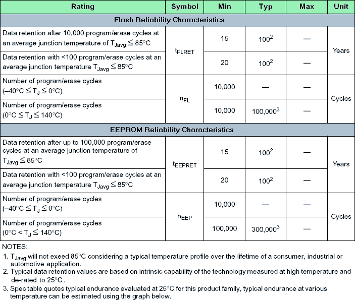
If EEPROM writes occur at room temperatures, each EEPROM cell is guaranteed to withstand 100,000 write cycles, and will typically endure 300,000 writes. At lower temperatures write operations are more likely to damage the device; if writing at less than 0°C, EEPROM cells are guaranteed to withstand only 10,000 write cycles.
Data retention
If a cell has been written to fewer than 100,000 times, you can expect the most recently written data to be retained for at least 15 years. If the device is operated at 25°C, it is likely that the data will be retained for about 100 years.
More detailed reliability specifications for the PDQ Board's nonvolatile memory, Flash and EEPROM, are provided by the following table (taken from the Freescale 9S12 Device Guide):

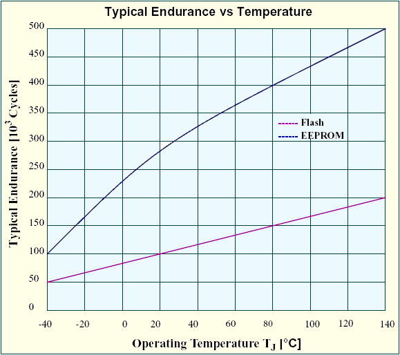
The number of write cycles before the EEPROM typically wears out depends on the processor's operating temperature, generally improving at warmer temperatures, as shown in Figure 1:

Typical EEPROM lifetime
EEPROM is intended to provide nonvolatile storage of configuration data and settings that do not need to change frequently. If an application program were to write to an EEPROM cell frequently it would quickly wear it out, limiting the lifetime of the product. On the other hand, if the C-language application program writes infrequently, the EEPROM should last longer than the product lifetime. You can expect individual EEPROM sectors (4-byte cells) to endure at least 100,000 write cycles, and typically several times that. The following table gives you a perspective on an EEPROM cell's expected lifetime for various write frequencies (assuming a worst case expected 100,000 write cycles to wear out):
| Time between writes | Expected lifetime |
|---|---|
0.03 sec | 50 minutes |
1 sec | 1 day |
1 min | 69 days |
10 min | 2 years |
1 hr | 11 years |
8 hr | 91 years |
As you can see, if a cell is written to an average of only once every few hours, perhaps in conjunction with instrument start-up or turn-off, the cell should last several decades.
Wear leveling for improved lifetime
Generally, only a few EEPROM variables are written to frequently, while the rest are rarely changed, causing particular cells to wear out long before the others. Wear leveling algorithms rotate the variables through the physical storage addresses so that all cells wear evenly. Using wear leveling you can greatly increase the lifetime of the device. For example, if only one variable receives the majority of write activity, rotating that variable through 100 memory cells increases the effective lifetime by a factor of 100.
Wear leveling spreads out the data evenly across the available EEPROM addresses over time. We'll do this by rotating the data throughout the addresses on a schedule.
There are various algorithms for "wear leveling" the cells of the EEPROM, so that they are all used evenly and wear out evenly. These algorithms all involve rotating your variable storage area throughout the EEPROM addresses, so that no single address is written to more than others. The process is complicated a bit by the need to make it robust with respect to power failures. After an unexpected reset, which might occur even during a write operation, the system needs to be able to identify the correct positions of the variables.
There are several published wear leveling algorithms for safe high endurance parameter storage in EEPROM. For example, Atmel recommends a rather complicated dual circular buffer scheme.
We'll describe a simpler scheme. Like all wear leveling algorithms it makes a trade-off among robustness, available memory, and wear leveling. In our trade off, we'll sacrifice about one half of the memory.
The PDQ Board's EEPROM area for the application's use comprises 384 bytes (or 96 cells) from 0x0680 to 0x07FF. We divide that into three regions: one contains status variables, another is the active variable area, and the third is an unused area to which the active variable area is periodically copied. The details are as follows:
- Three status cells, each of 4 bytes, are located at 0x0680-0x068B. Two status cells are duplicates of each other, so that write errors in either of them can be detected. A third cell is reserved for future use. Each of the two identical status cells holds two variables, a 16-bit month:day (or possibly only the month for a simple shift only once per month) representing the last time the variable area was shifted, and a 16-bit base address of the active variable area. Valid base addresses are 4-byte aligned addresses from 0x068C to 0x07FC.
- An active variable area of 184 bytes (or 46 cells), starting at the base address, and wrapping around the 0x07FF/0x068C border if needed.
- An inactive area, of 188 bytes (or 47 cells).
During normal operation, the application program uses variables in the active variable area of the EEPROM. The application program addresses variables using a variable offset, from 0 to 187 which it adds to the active variable area base address. When it does the addition, it must wrap around the 0x07FF address if necessary.
At startup, a routine checks the real time clock, and compares the date to the last EEPROM shift date. If enough time has passed it shifts the EEPROM variables and updates the base address. It does this by first copying the active variable area into the unused area, then if no errors occurred it updates the base address.
Use one routine for Read_EEPROM_Vars and another routine for Write_EEPROM_Vars. Then the application can read them all, and only periodically write them.
- The shift routine should be robust with respect to lack of production time initialization of the EEPROM. That is, when first run, it should initialize the status cell.
- The EEPROM variable area is shifted and the offset is updated only during the start-up initialization routine, before other tasks are activated, so that other parts of the application program can not write to the EEPROM during the shift operation.
- All users of the EEPROM must add the offset to the EEPROM address.
- All EEPROM read/writes must be 4-byte aligned. Doing so greatly simplifies the read/write operations by removing the need to check that the variable might be at the wrap around border of the active variable area.
For more information:
See also → Failure and Run-Time Error Recovery
