Digital I/O - Hardware Interfacing
On this page you'll learn how to interface external hardware devices to the PDQ Board's digital I/O pins. The processor’s digital input/output pins are brought out to the Digital I/O header so you can easily connect to them. You can use them to directly drive LEDs, relays, transistors, opto-isolators or other digital logic devices. But please be careful – whenever these outputs are connected to external devices you must stay within the voltage and current capabilities of the output pins.
Electrical characteristics of the 9S12 processor’s I/O ports
The electrical characteristics of the processor’s digital I/O signals are specified in detail in Appendix A of the Motorola HCS12 Device Guide document. A table lists the 5V I/O Characteristics of the processor.
AN2434: Input/Output (I/O) Pin Drivers on Freescale 9S12/HCS12 Family MCUs
AN2727: Designing Hardware for the Freescale 9S12/HCS12 D-Family
Input pin logic levels and threshold voltages
Pins on the HCS12 configured as digital inputs are guaranteed to report a logical high if the input voltage is greater than 0.65 times the supply voltage, or 3.25 Volts. They will always report a logical low if the input voltage is less than 0.35 times the supply voltage, or 1.75 Volt. Input voltages between 1.75 and 3.25 volts are indeterminate; they may be read as either high or low by the processor, depending on the exact value of the trigger, or threshold between logic high and logic low. The trigger voltage can lie anywhere within the 1.75 – 3.75 V gap, and is typically around 2.5V
9S12 input pin hysteresis
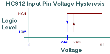
Further, each input/output pin exhibits a little hysteresis provided by weak pullup and pulldown transistors on the input pins. The consequence of this hysteresis is that the threshold between a logic high and a logic low depends on whether the input voltage is rising or falling. The following diagram shows the measured threshold for a single pin.
The 0.14V gap between the rising and falling thresholds provides some noise immunity and prevents chatter on the pin during voltage transitions. When the input voltage rises from a logic 0 toward a logic 1 level, the logic 1 is recognized when the voltage rises to 2.582 volts. Negative going noise on the input voltage will not cause a false transition back to a logic 0 unless it is greater than 0.14V. Likewise, during a logic 1 to logic 0 transition, the input is protected against positive going noise spikes of less than 0.14V. The actual threshold values and degree of hysteresis will vary from pin to pin.
The hysteretic input works together with any source impedance driving the pin to provide some immunity against noise and to debounce the input signal.
9S12 output pin full drive and partial drive modes
Pins on the 9S12/HCS12 come up in the standard full drive mode, and can be configured for partial drive to save a small amount of bias current. Full drive mode is recommended for most applications. No action is required to obtain full drive, as this is the default condition after a reset.
Full-drive 9S12/HCS12 pins configured as digital outputs in the high state can maintain the output voltage within 0.8 V of the positive supply if 10 mA or less is being drawn from the pin. In the low state, full-drive digital outputs can keep the voltage below 0.8 V while sinking up to 10 mA of current. Load circuitry that requires significant current to be sourced or sunk by the digital output should include external resistors to ensure that the absolute maximum rating of 25 mA per output pin is never exceeded.
9S12 output pin V-I electrical characteristics
The output pins of the HCS12/9S12 are similar in electrical characteristics to the SN54/74HC digital logic family. The digital outputs can source or sink up to 25 mA, although they are specified at ±10mA. A valid logic high level is between VOH = VDD and VOH = 0.65 VDD, and a valid low level is between VOL =VSS = 0 V and VOL =VSS + 0.35 VDD. As the output is loaded, the VOL and VOH levels rise or fall. It is often useful to know just how much to expect the VOL and VOH levels to degrade with current.
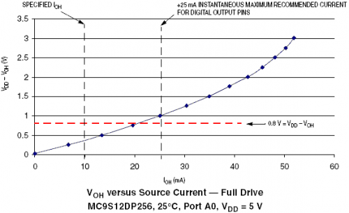
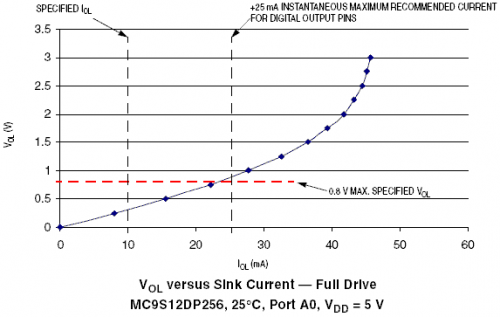
When the pins are operated with full drive capability (their default state) their output resistance is approximately 40Ω. That is, for currents of less than 10 mA the voltage change is linear with current; it can be modeled as a voltage source of either zero or five volts and an equivalent series resistance of 40 ohms 1). At greater output currents the resistance increases gradually, but the 40 ohm approximation holds good up through the 25 mA maximum. At this current the voltage degradation of the VOL or VOH is about 1 volt. The following graphs illustrate the variation.
The graphs (or the simpler 40Ω value) can be used to choose component values for particular circuits. For example if we wish to use an I/O pin to drive a light-emitting diode, we would place the LED in series with a resistor and connect them between an output pin and ground. The resistor limits the current into the LED. From the LED datasheet we note that its forward voltage at a current of 10 mA is specified to be 2.2 V. What should the resistor value be? We calculate it as,
Consulting the VOH vs I curve for the I/O pin, we find that VOH = 4.6 V at 10 mA. Plugging 4.6V into the above equation results in a calculated external resistance of 240 ohms.
You may either source current to the LED, or sink current from it, as shown in the following circuit. When sourcing current to it an active high turns ON the LED; when sinking current an active low turns ON the LED.
9S12 output pin voltage vs current in full drive mode
The following graphs show that the resistance of an output pin in either the high or low state is approximately 40 ohms for currents to the maximum of 25 mA.
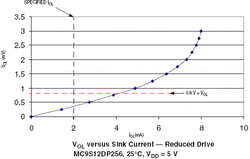
9S12 output pin voltage vs current in reduced drive mode
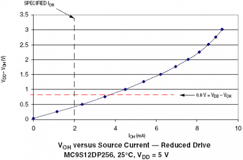
The following graphs show that in reduced drive mode the resistance of an output pin is approximately 200 ohms in either the high or low state.
Protecting the 9S12 input and output pins
These digital output pins are very useful because they can directly drive a wide range of devices. Nevertheless, any circuitry connected to the processor should take care to:
- Prevent excessive voltage levels at the pin; and,
- Prevent excessively great currents.
We’ll address each of these concerns in turn.
Preventing excessive voltages
The HCS12 family MCUs include ESD (Electrostatic Discharge Protection) structures on all I/O pins. They consist of internal diodes that conduct current from the input pin to the supply or ground rails in the event that the input pin voltage exceeds the supply range. The ESD structures are described in the Freescale Pin Driver Datasheet under the heading ESD Structures. However, you should not rely on the internal diodes to prevent damage from excessive voltage.
Excessive voltages are prevented by ensuring that voltages of less than a diode drop below VSS (that is, -0.6 V below ground) or greater than a diode drop above VDD (that is, 5.0 + 0.6 V) are never applied to the processor. For some applications, particularly when driving inductive loads such as relays, you may need to provide Schottky diode clamps between the pin and VDD and between the pin and ground. All digital I/O pins on the processor have inherent diode clamps to the processor’s ground voltage, VSS, but it is best not to rely on these. If there is the possibility of the output pin being driven to a negative voltage level it is better to prevent excessive power dissipation in the processor package by externally clamping the voltage to ground (VSS) with a Schottky diode.
The HCS12 datasheets warn that if current is injected into a pin by excessive voltage the current must be limited to less than ± 2.5mA; otherwise there may be long term reliability problems.
Preventing excessive currents
The current into or out of any pin on the MCHCS12 should also be limited to prevent damage. The specified maximum instantaneous current is 25 mA into or out of any one pin at a time. In driving more than one pin at a time it is necessary to stay within the processor’s maximum power dissipation. Unfortunately, Motorola doesn’t specify exactly what this maximum is, but we recommend that you don’t exceed a total of 250 mW for all processor I/O pins combined if you are operating within the commercial temperature range (0 to 70 degrees centigrade). The chip’s total power dissipation is the sum of its internal power (which varies from device to device so much that it can only be determined by actually measuring it, but which is specified at less than 325 mW) and the power associated with the I/O pins. Pin currents must be limited using external resistors.
See also → Pulse Width Modulated I/O

